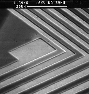
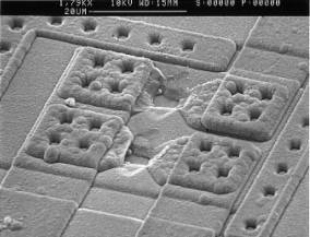
SEM photo of a planar microcoil (tilted view).
This picture shows a detail of a microcoil for cryogenic applications, to be fabricated by lift-off.
The large pad is the end contact of the coil, which will be connected through a second-level metallization.
The lines are 4 µm wide, separated by a 4 µm gap. The sample has been tilted by 45 degrees in order to show the photoresist thickness, which is 0.8 µm.
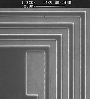
SEM photo of planar microcoil (top view).
Same picture as above. Here the ratio between linewidth and line roughness is well visible, and the overall resolution can be evaluated.
For this pattern the resolution is nominally set to 1 µm. This means that the proper focusing lens for this resolution has been selected. However, the actual resolution (if a thin resist and accurate process control is made) is better than 1 µm, as shown in the photographs below.
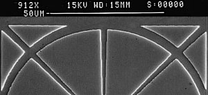
Detail of a test pattern for round shapes
The width of each line decreases toward the centre. The central line has a stair like appearance. The size of each step in the edges is 0.2 µm, equivalent to the mesh size of the "electronic grid" of the system.
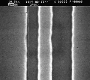
Detail of line edge roughness.
The two dark areas in this high magnification SEM photograph are respectively 1.2 and 2.4 µm wide. They are laser-written on 0.8 micron thick resist.
The average edge roughness is within 0.2 µm (peak to peak), as indicated by the two vertical white rulers, which are 200 nm apart.
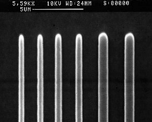
Test pattern for 0.7 micron nominal resolution.
This photograph shows a resolution test for 0.7 µm
nominal resolution. The lines of each couple are respectively 0.5, 0.7 and
1 µm wide. The pattern is negative, on 0.5 µm thick positive resist.
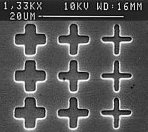
Detail of an array of crosses with different linewidth.
The arms are respectively 2.4, 1.8 and 1.2 µm
wide.
The pattern is opened in 0.8 µm positive resist.
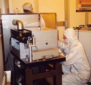
Installation at customer's site
The body of the writing unit is placed on a vibration damping legs frame. It hosts the laser source, the microtranslation xyz stages, the interferometer, the beam conditioning optics and other electro-optical devices used for pattern generation. A 19" rack, located nearby, hosts the control electronics and the user interface. The compact design os the LaserWriter results in a reduced footprint, for an easy installation even in a small research clean-room.
The system is CE-marked: it complies with the European laws for safety and EMI control. Safety compliance for each country can be tested and included. Assembling is made in clean-room.
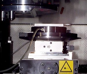
Detail of the work chamber.
The y and z translation stages can be seen in the lower part of the photo (respectively dark and white). The round dark part in the centre is the substrate holder, and hosts the interferometer mirrors. The wheel visible on the the upper-left side allocates aset of focusing lenses. These can be remotely selected, according to the desired resolution for the writing process or during sample observation and surface metrology operations.
Trimming on a silicon wafer.
This photogragh shows an application of the LaserWriter customized for surface ablation. The pulse from a Nd-YAG or Excimer laser source is precisely aimed at the target through the LaserWriter. The 5 µm square holes created on the surface correspond to the blowing of conductive links included in the microcircuit for tromming purposes. Pointing can be made manually or can be driven by an image processing system.
(Wafer by ST-Microelectronics).

This photogragh shows 40GHz devices made by direct patterning on the final substrate.
The photograph shows a microstrip device patterned on a galvanoplated RT-Duroid(TM).